MICROPROG
Die Website wird ausschließlich auf Englisch angeboten.
The component "microprog" demonstrates, how the Mixed Instruction Processor Set (MIPS) instruction set can be implemented by a hardware structure and visualises the dynamic behaviour of the datapath. The component simulates the execution of MIPS instructions and shows the data transfers within the hardware structure.
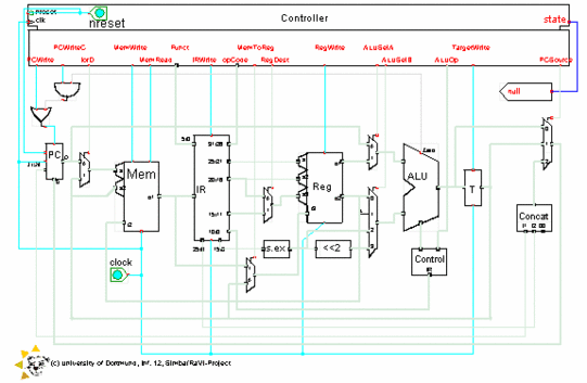
The hardware structure specified in this component is a multicycle implementation of the MIPS-processor. Implying that the hardware structure uses more than one clock cycle to complete the execution of a single instruction. The implementation is widely identical to the one described in chaper 5.4 of the book "Computer Organization and Design" from Hennessy & Patterson. A schematic of the hardware structure is given in illustration 1.

The schematic of the component "microprog" represents the hardware structure and at the same time it defines the appearance of the visualization. It shows the controller, the program counter "PC" with the write control gate "B", the memory unit "Mem", the instruction register "IR", the sign-extension unit "s.ex", the register file "Reg", the arithmetic and logical unit "ALU", the ALU control gate "Control", the ALU out register "T" and the gate "Concat" which has the task to build the jump address. | ||
The content of the memory unit, the current MIPS instructions, and the content of the register file are not determined by the component. The user can change them interactively during the visualization. The instructions in the memory unit can be entered either as assembler code or as 32bit strings. The register values of the register file have to be entered as 32bit strings. The default memory content and the default register file content are given in the file "mem.bin" and "reg.bin" respectively. These files are situated in the RaVi directory and will be loaded automatically during the start of the component. |

