CACHEPROTOCOL
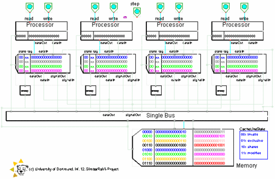
The component "cacheprotocol" demonstrates, how the MESI protocol can be used as a multi-processor cache coherence protocol by visualizing the dynamic process of the MESI protocol. The component represent a multi-processor system with a shared memory, four processors, their corresponding caches and a snooping bus. Visualizing the dynamic process of the protocol means that depending on different read and write requests of the processors the component shows the signal and data transfers between the individual caches and the memory. Moreover it visualizes the state transitions of the addressed cache blocks. In illustration 1 you can see a picture of the component structure.
The Modified-Exclusive-Shared-Invalid (MESI) protocol is an example for a write invalidate protocol and ensures the cache coherence in a multi-processor system. The realized protocol process of the component is based on the protocol description in chaper 9 of the book "Computer Organization & Design, The Hardware/Software Interface " from Hennessy & Patterson. For a visualization of the cache state transitions of the MESI protocol please have a look to the RaVi component "mesi".
The book of Hennessy & Patterson quotes no special hardware structure for the implementation of the MESI protocol. For learning the basic concepts of the protocol we have decided to visualizes the MESI protocol process and therefore we have described the elements on a higher abstraction level. Only that kind of behavior is specified by the component which is necessary for the process of the protocol. Additional functionality, for example of the cache memories or the processors, is not implemented. At this point it is important to mention, that the structure described in this component is not a complete hardware structure for the implementation of the MESI protocol.

The illustration above shows the structure of the component. At the top you can see the four processors of the multi-processor system. Within the icon of each processor a memory buffer is displayed. This memory buffer is addressed whenever the processor issues a read or a write request.
The corresponding cache memory of a processor is situated directly under the processor. All cache memories are implemented as write-back caches. They show their current cache lines along with the state of each cache line. In the lower right corner of the illustration you will find a caption with the cache line state codes and their meanings.
The memory unit, so called "Memory", you will find at the bottom of the structure. It displays its current content, the memory blocks.
The processors, the cache memories and the memory unit are connected by a snooping bus, named "Single Bus". We have avoided implementing a bus arbiter, because the component should not be too complex. Only one unit can use the bus at a given time.
The light blue lines, as shown in the illustration, represent the control and data signals between the units. If they are colored in light blue, they are not relevant in the actual visualization step. The relevant signals in a step will be highlighted with different colors later during the visualisation.
With the two switchs "read" and "write" at the top of each processor and the single switch "step" the user can control the application flow of the visualisation.
The switch "step" represents a single step of the visualisation. It is realized by a manual clock signal and every clock edge the component goes on to the next step of the visualization.
For showing how the MESI protocol works the user should sequentially issue read and write requests from different processors. Each request are followed by some visualization steps, which show the resulting data and signal transfers between the processors, their corresponding caches and the memory. The switches "read" and "write" respectively issue a read and write request of the processor. A read request for example is issued, if the switch "read" has the output value '1'. The output value '0' stands for a disabled request.
The contents of the memory unit and of each processor are not determined by the component. The user can change them interactively during the visualisation. The values can be entered as 16bit strings. The files "memmesi.bin" and "processor.bin" contain the default memory content and the default content of each processor. These files are situated in the RaVi directory and will be loaded automatically during the start of the component.

